The Strategic Role of BN Materials in Semiconductor Manufacturing
In semiconductor manufacturing, consistency is everything. Every step, from wafer production to final packaging, demands tight control over temperature, purity, and structural stability. At the center of this complex landscape, materials engineering quietly dictates the pace, and boron nitride (BN) materials are increasingly making their presence known.
What Makes BN Materials So Valuable?
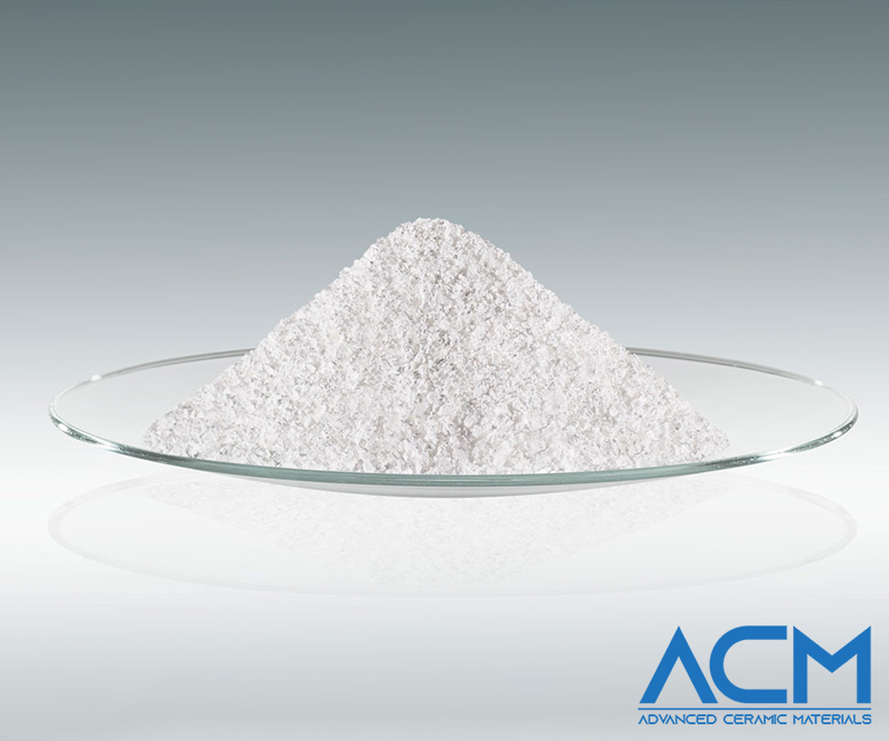
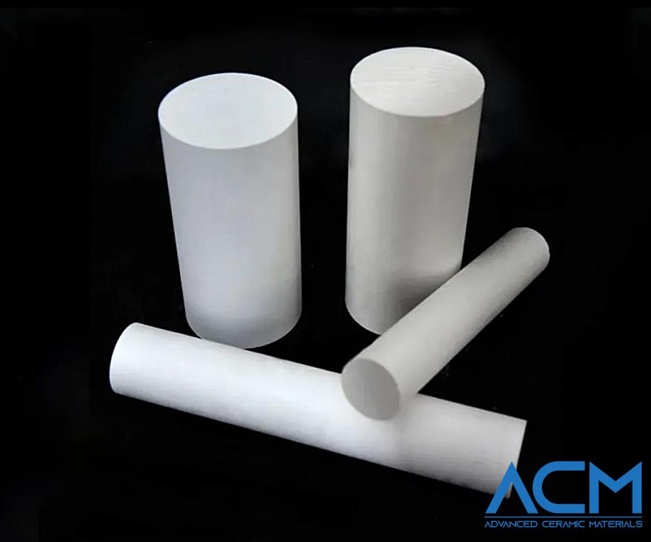
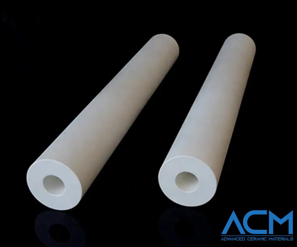
BN, or boron nitride, is a compound made from boron and nitrogen atoms in a hexagonal or amorphous arrangement.

In practice, we typically encounter two types in the semiconductor world:
-
Hexagonal BN (h-BN): Structurally similar to graphite, offering high thermal conductivity, electrical insulation, and chemical inertness.
-
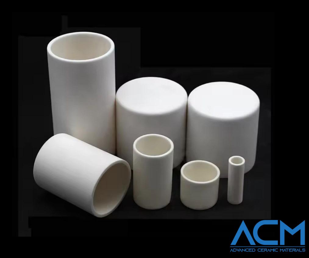
Pyrolytic BN (PBN): Produced via chemical vapor deposition (CVD), it delivers extreme purity and a dense, uniform microstructure.
These properties are not just nice to have—they’re essential for precision manufacturing environments where contamination, thermal mismatch, or structural failure can cost millions.
Where BN Materials Fit Into the Fab
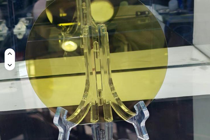
1. Wafer Handling and Support
BN components are commonly used to support or clamp semiconductor wafers during crystal growth or other high-temperature processes. The material’s thermal stability allows it to maintain shape and alignment at temperatures exceeding 1800°C. Meanwhile, its low thermal expansion minimizes mechanical stress on the wafer, protecting fragile substrates from microcracking or deformation.

2. Ion Implantation Systems
Ion implantation is all about control. BN parts—typically insulators or beamline components—help maintain beam stability and reduce particle scattering. Their high dielectric strength makes them ideal for withstanding the intense electric fields used during implantation, while their chemical stability ensures long-term durability even in plasma-rich environments.
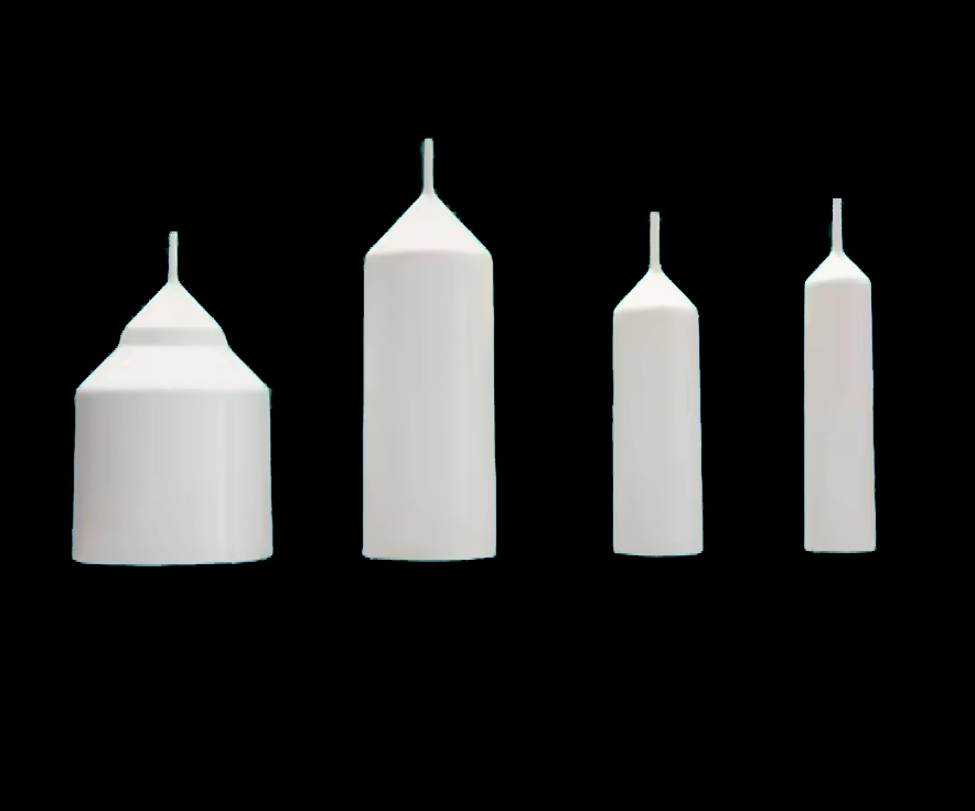
3. Thermal Process Fixtures
Heat treatment stages (oxidation, annealing, diffusion) require materials that can withstand prolonged exposure to high temperatures and reactive gases. BN jigs and plates not only hold up under extreme conditions but also do so without contaminating the environment—something that even advanced ceramics like alumina can’t always guarantee.
Why BN Offers More Than Just "Toughness"
BN materials don't just survive tough environments—they improve them.
Extending Equipment Lifespan
Thanks to its wear resistance and corrosion resistance, BN reduces the rate at which components erode or degrade. Over time, this lowers the total cost of ownership for fab tools, minimizes downtime, and makes predictive maintenance far more manageable.
Purity Matters
PBN, in particular, offers chemical purity levels above 99.99%. This drastically lowers the risk of metallic or particulate contamination during wafer processing, one of the most common sources of yield loss in front-end semiconductor fabs.
Process Stability
BN’s thermal conductivity helps dissipate heat evenly during high-energy steps like rapid thermal annealing or etching. Combined with a coefficient of thermal expansion (CTE) close to that of silicon and sapphire, this makes BN an ideal structural match for semiconductor substrates.
The Road Ahead: Where BN Is Poised to Grow
Quantum Chip Manufacturing
As we move into cryogenic and low-noise regimes, BN’s insulating and thermal properties make it a natural fit for quantum chip packaging and thermal management. Its chemical stability at near-zero Kelvin is also an area of active research.
Deep-UV Optoelectronics
BN’s wide bandgap and UV transparency are opening up new opportunities in the deep ultraviolet (DUV) space. From high-power light sources to UV detectors, BN components help manage heat and preserve optical clarity where traditional materials would degrade.
Emerging Frontiers: Flex and Nano
With the rise of flexible and wearable electronics, BN is being explored as a substrate and protective layer. Its combination of flexibility, strength, and thermal resistance makes it a candidate for next-gen sensors, displays, and conformal devices.
Final Thoughts
BN materials may not be the most talked-about component in a semiconductor fab, but their impact is anything but marginal. From holding wafers steady during high-heat processes to enabling breakthroughs in quantum computing, BN quietly but powerfully supports progress at every scale.
At Advanced Ceramic Materials (ACM), we’ve worked with hundreds of fabs, research labs, and system integrators to supply high-purity BN products—including PBN crucibles, custom-shaped thermal jigs, and precision-machined h-BN components. Whether you're building for today’s nodes or tomorrow’s quantum systems, BN may be the material you didn’t know you needed.
Explore our full materials offering here: https://www.preciseceramic.com/products.html
{{item.content}}
LEVE A REPLY
{{item.children[0].content}}
{{item.content}}
LEAVE A REPLY
SUBSCRIBE OUR NEWSLETTER
- What Are Structural Ceramics and Why Are They Important?
- N-Type and Semi-Insulating SiC: Choosing the Right Material for Power and RF Devices
- Alumina Bearing Balls: How a Tiny Ceramic Sphere Is Redefining Precision in Extreme Environments
- Thermal Management in Power Electronics with Hexagonal Boron Nitride
- Why Alumina Grinding Balls Are Replacing Steel Across Multiple Industries
 Guide to Alumina Grinding Balls: Properties, Applications, and Selection
Alumina grinding balls are dense ceramic spheres made from high-purity aluminum oxide (Al₂O₃). Known for their hardness, chemical resistance, and thermal stability, they serve as essential grinding media in industries that rely on consistent, clean, and efficient particle size reduction.
READ MORE >
Guide to Alumina Grinding Balls: Properties, Applications, and Selection
Alumina grinding balls are dense ceramic spheres made from high-purity aluminum oxide (Al₂O₃). Known for their hardness, chemical resistance, and thermal stability, they serve as essential grinding media in industries that rely on consistent, clean, and efficient particle size reduction.
READ MORE >