


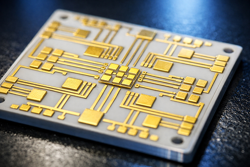
How PBN Crucibles Ensure the Quality of GaN & SiC Epitaxial Materials
Abstract: In the atomic-scale world of GaN HEMTs and SiC power devices, the vessel that holds the source materials is not just a container; it is the foundational determinant of epitaxial film purity. Trace contaminants from a crucible can incorporate as fatal defects. This article details why Pyrolytic Boron Nitride (PBN) has become the non-negotiable material for MOCVD and MBE components, examining its unique combination of ultra-high purity, thermal management, and non-wetting properties. We explore its critical applications across GaN and SiC platforms and outline the engineering required to manufacture reliable, complex PBN shapes for leading-edge epitaxy tools.
Introduction: When a Single Atom is a Defect
The performance frontier for RF GaN and high-voltage SiC devices is defined by crystalline perfection. A single silicon vacancy in SiC, or an unintentional oxygen impurity in a GaN channel, can degrade electron mobility, breakdown voltage, and ultimately, device yield and reliability. These defects don't just originate from the source gases or silicon carbide boule; they can leach directly from the crucibles, boats, and liners inside the epitaxial reactor.
The challenge is twofold: extreme chemical inertness to prevent reaction with molten metals (like Ga) or aggressive precursors (like NH3), and minimal outgassing to maintain an ultra-high vacuum (UHV) in MBE or a controlled atmosphere in MOCVD. Traditional materials fail one or both tests, making Pyrolytic Boron Nitride (PBN) not a premium choice, but the only viable one for volume production of high-end devices.
The PBN Advantage: A Property Set Without Equal
PBN is not sintered or pressed; it is deposited via Chemical Vapor Deposition (CVD) from boron halide and ammonia precursors. This process yields a material with a unique constellation of properties critical for epitaxial growth.
| Property | PBN Characteristic | Direct Impact on Epitaxy | Why Alternatives Fail |
|---|---|---|---|
| Purity | >99.99% (4N) typical, with metallic impurities in low ppm. | Eliminates a primary source of dopant contamination (e.g., Fe, Cu, Al) that creates deep-level traps, killing device performance. | Graphite: Porous, traps moisture/salts, high inherent impurities. Quartz (SiO₂): Releases oxygen and sodium, poisons III-V growth. Alumina (Al₂O₃): Source of aluminum contamination, reacts with many melts. |
| Anisotropic Thermal Conductivity | High in-plane (~400 W/m·K), low through-plane (~2 W/m·K). | Provides excellent lateral temperature uniformity for melts (like Ga) while acting as a thermal barrier vertically, enabling precise thermal gradients. | Isotropic materials cannot provide this directional control, leading to hot spots and uneven evaporation/ sublimation rates. |
| Outgassing & Vacuum Compatibility | Extremely low, stable under high vacuum and temperatures up to 1800°C. | Essential for maintaining the 10⁻¹⁰ Torr base pressure required by MBE. Prevents process drift and chamber memory effects in MOCVD. | Porous graphite is a notorious gas reservoir. Ceramics can release bound water and gases at temperature. |
| Non-Wetting & Chemical Inertness | Does not react with or wet by most molten metals (Ga, Al, Si) or salts. | Precludes alloying with the source material. Crucible can be reused without build-up or degradation, ensuring consistent evaporation rates. | Many metals wet and alloy with graphite or quartz, consuming the crucible and altering source composition. |
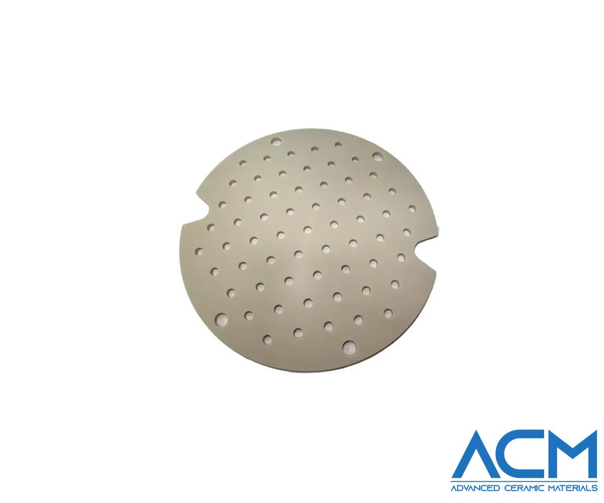
Application Scenarios: Where PBN is Mission-Critical
1. GaN MOCVD: The Reactor Liner and Injector
In GaN-on-Si or Sapphire MOCVD, the reactor walls are exposed to hot, ammonia-rich gases. A standard quartz liner would slowly etch and release silicon and oxygen into the process stream.
-
PBN's Role: A PBN liner or coated graphite susceptor creates an inert barrier. It prevents silicon autodoping (critical for insulating buffer layers on silicon substrates) and eliminates oxygen contamination that would form compensating centers in the GaN layer, directly impacting HEMT sheet resistance and LED efficiency.
2. SiC Vapor Phase Epitaxy: The Coated Graphite Carrier
SiC epitaxy at >1600°C is one of the most hostile thin-film environments. Pure graphite parts outgas hydrocarbons and can react with the Si/C precursor gases.
-
PBN's Role: A dense, crack-free PBN coating is CVD-deposited onto precision-machined graphite carriers (boats, pedestals). This coating preserves the graphite's structural strength and thermal properties while presenting a perfectly inert PBN surface to the SiC growth environment, enabling high-purity, homoepitaxial layers for 1200V+ power devices.
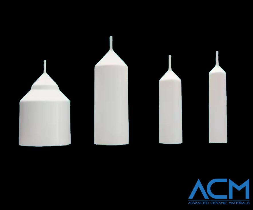
3. Molecular Beam Epitaxy (MBE: The Effusion Cell Crucible
MBE demands the ultimate in vacuum integrity and source material purity. The effusion cell crucible holds the elemental source (e.g., Ga, Al) and must heat it uniformly without contamination.
-
PBN's Role: Deep-drawn PBN crucibles (K-cells) are the universal standard. Their low outgassing preserves UHV. Their non-wetting property allows complete emptying of the source, maximizing material use and providing a consistent evaporation flux over the cell's entire lifespan, which is critical for growing complex multilayer structures with precise compositions.
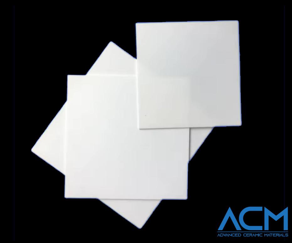
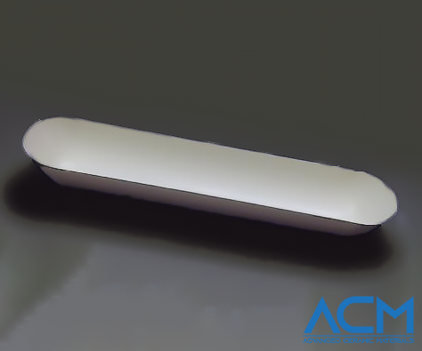
The Manufacturing Edge: Beyond the Blank
Supplying a usable PBN component is an engineering discipline in itself. At Advanced Ceramic Materials (ACM), our capability is defined by control over the entire CVD process:
-
Precision Deposition: We control the CVD parameters to tailor the degree of anisotropy, crystallographic orientation, and density of the PBN to the application (e.g., more isotropic for coatings, highly anisotropic for high-heat-flux liners).
-
Complex Shape Fabrication: Through a combination of mandrel-based CVD forming and precision machining, we produce components far beyond simple boats: complex injectors, shrouds, and custom-shaped liners that match the exact geometry of leading OEM reactor chambers.
-
Certification & Traceability: Every lot of raw material and finished component is tracked. We provide certification for key properties like bulk purity, density, and high-temperature vacuum weight loss, giving you the data needed for your own process qualification.

Conclusion
In the quest for higher frequency, higher power, and higher efficiency devices, the margin for error at the materials level has vanished. The crucible is no longer a passive container; it is an active process-determining component.
Choosing PBN is not a cost decision; it is a yield and performance decision. It is the deliberate elimination of a major, controllable source of contamination and process variability. For fabs pushing the limits of GaN and SiC technology, the consistent quality of epitaxial layers begins with the purity and integrity of the PBN components within the growth chamber.
Is your epitaxial process limited by source or chamber contamination?
Contact our PBN engineering team at ACM. Share your reactor model and process challenges. We will analyze compatibility and provide a proposal for PBN components designed to maximize the purity and consistency of your GaN or SiC epitaxial growth.
{{item.content}}
LEVE A REPLY
{{item.children[0].content}}
{{item.content}}
LEAVE A REPLY
SUBSCRIBE OUR NEWSLETTER
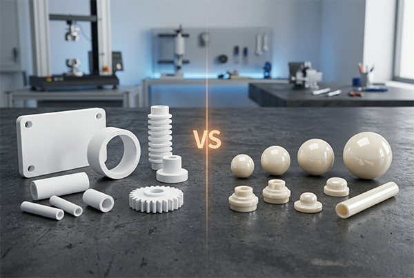
- Oxide, Sulfide, or Phosphate? A Supplier's Guide to Solid-State Electrolyte Ceramics
- Alumina vs. Zirconia Ceramics: The Engineering Blueprint for Material Selection
- Case Study: Sub-Millimeter Sapphire Tubes for High Voltage Discharge Applications
- Alumina Powder (Al2O3): A Technical Guide to Grades, Properties, and Applications
- Ceramic Machining: Essential Techniques and Processes for Precise Components

 AlN Ceramic Substrates for UV-LED and Mini LED Packaging
AlN ceramic substrates deliver 170-230 W/mK thermal conductivity for UV-LED and Mini LED packaging. Compare DPC vs thin film metallization, CTE matching to GaN/Si, and 85/85 reliability data. Selection guide included.
READ MORE >
AlN Ceramic Substrates for UV-LED and Mini LED Packaging
AlN ceramic substrates deliver 170-230 W/mK thermal conductivity for UV-LED and Mini LED packaging. Compare DPC vs thin film metallization, CTE matching to GaN/Si, and 85/85 reliability data. Selection guide included.
READ MORE >
 Alumina vs. Zirconia Ceramics: The Engineering Blueprint for Material Selection
This article compares their physical properties, real-world trade-offs, and cost-benefit realities to help you select the right ceramic for your operating environment.
READ MORE >
Alumina vs. Zirconia Ceramics: The Engineering Blueprint for Material Selection
This article compares their physical properties, real-world trade-offs, and cost-benefit realities to help you select the right ceramic for your operating environment.
READ MORE >
 Oxide, Sulfide, or Phosphate? A Supplier's Guide to Solid-State Electrolyte Ceramics
Oxide, sulfide, or phosphate? A practical guide to solid-state electrolyte ceramics from a supplier who handles them daily. Compare LLZO, LATP, and LGPS on conductivity, processing, stability, and real-world viability.
READ MORE >
Oxide, Sulfide, or Phosphate? A Supplier's Guide to Solid-State Electrolyte Ceramics
Oxide, sulfide, or phosphate? A practical guide to solid-state electrolyte ceramics from a supplier who handles them daily. Compare LLZO, LATP, and LGPS on conductivity, processing, stability, and real-world viability.
READ MORE >