




How to Choose a Metal Coated Ceramic Substrate
Choosing a metal-coated ceramic substrate requires two linked decisions. The ceramic controls insulation, heat flow, stiffness, and resistance to thermal cycling. The metal system controls current carrying, soldering or sintering, wire bonding, corrosion behavior, and pattern resolution. Selecting the ceramic first and treating the coating as a generic finish often creates a substrate that looks acceptable on a drawing but does not match the assembly process.
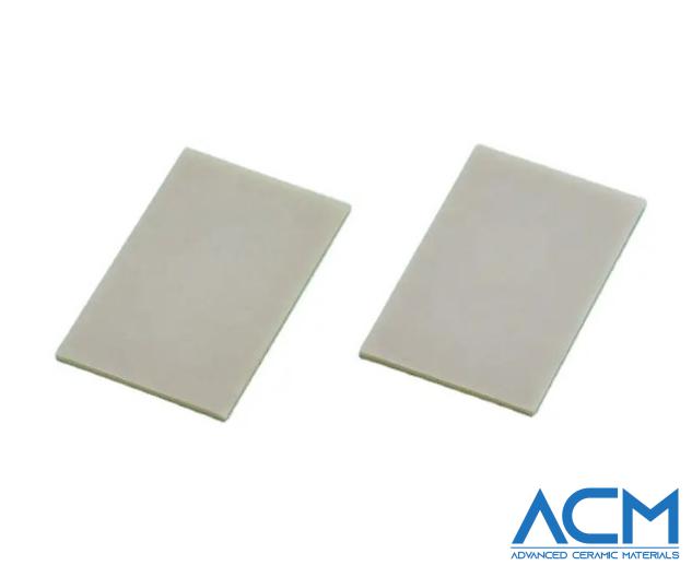
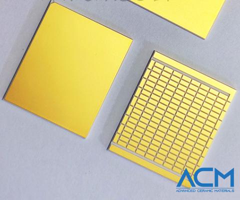
The practical starting point is the complete stack: semiconductor or device, die-attach material, metal finish, conductor, ceramic, backside metal, baseplate, and coolant path. ACM's metal-coated ceramic substrate range includes alumina and aluminum nitride substrates with nickel, palladium, gold, and silver surface systems. The correct configuration depends on how the substrate will be assembled and tested.
Choose the Ceramic Based on Thermal and Mechanical Load
|
Ceramic |
Useful strengths |
Important limitations |
Typical selection logic |
|
Established processing, electrical insulation, broad availability, cost control |
Lower thermal conductivity than AlN and high-performance Si3N4 |
Suitable when heat flux and cycling severity are moderate or cost and process maturity dominate |
|
|
High thermal conductivity, electrical insulation, CTE closer to silicon than alumina |
More sensitive to processing and moisture chemistry; lower toughness than Si3N4 grades used for power substrates |
Suitable when junction-to-case thermal resistance is the main constraint |
|
|
High flexural strength and fracture toughness, strong thermal-cycling performance, thin-section potential |
Thermal conductivity is generally below high-conductivity AlN, though grade dependent |
Suitable when mechanical reliability and repeated power cycling dominate |
For standard AlN product data, review ACM's aluminum nitride substrates. The listed thermal conductivity exceeds 170 W/m·K for that product, but a design should use the supplier's grade-specific guaranteed value rather than a generic handbook number.
Ceramic thickness belongs in the same decision. Lower thickness reduces one part of through-plane thermal resistance, but it also affects dielectric margin, handling yield, warpage, stiffness, and resistance to copper-induced stress. A high-conductivity material is not automatically the lowest-risk option if the chosen thickness and conductor geometry create excessive mechanical strain.
Select the Metal System From the Joining Process
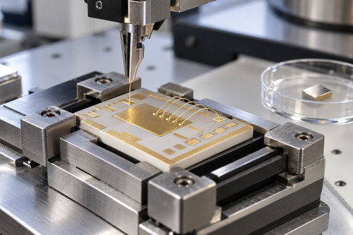
The final metal surface must match the next manufacturing step. "Gold plated" alone is incomplete because the underlayer, gold type, thickness, porosity, and storage condition affect solderability and wire bonding. The buyer should identify the actual solder, sinter paste, wire material, bonding method, peak temperature, reflow count, and cleanliness requirement.
|
Surface system |
Why it is used |
Questions to resolve before ordering |
|
Nickel and gold |
Nickel acts as a diffusion barrier; gold protects the surface and can support joining or bonding |
Electrolytic or immersion process, hard or soft gold, thickness, solder system, wire material, and shelf-life requirement |
|
Nickel palladium gold |
Adds a palladium layer between nickel and gold and can provide a versatile assembly surface |
Exact stack and thickness, gold or aluminum wire bonding, solder qualification, and whether the process is ENEPIG or another plated stack |
|
Silver |
High electrical and thermal conductivity and compatibility with selected silver joining processes |
Tarnish control, sulfur exposure, ionic migration risk, storage packaging, and final joining chemistry |
|
Bare or protected copper |
High current capacity and direct use with selected solder or sinter processes |
Oxidation control, surface preparation, copper roughness, pattern thickness, and time between cleaning and assembly |
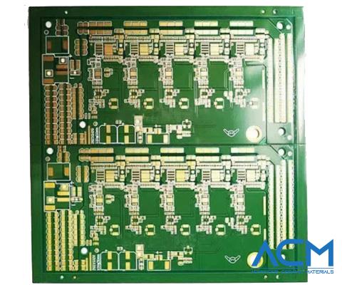
Examples in the ACM range include a nickel-gold plated alumina substrate, a nickel-palladium-gold plated AlN substrate, and a silver-plated AlN circuit board. These examples show available configurations; they should not be treated as interchangeable finishes.
Determine Whether the Metal Is a Finish or a Conductor
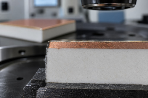
A thin plated finish serves a different purpose from a thick copper conductor. The drawing should distinguish the adhesion or barrier layer, the current-carrying layer, and the final surface finish. For power circuits, conductor thickness affects current density, heat spreading, etch geometry, and stress. For fine-pitch circuits, pattern resolution and edge definition may matter more than maximum copper thickness.
Do not compare metal thickness without also comparing line width, spacing, copper balance, ceramic thickness, and operating temperature. Thick or highly asymmetric metal can bend a thin substrate or increase interfacial stress during cycling. Symmetric designs may help control curvature, but the electrical layout may prevent perfect symmetry. Warpage therefore needs a drawing limit and a defined measurement state.
Specify the Circuit and Mechanical Layout Together
- Overall substrate size, ceramic thickness, and individual or master-card delivery format
- Top and backside metal coverage, thickness, and pattern alignment
- Minimum line width and spacing, isolation distance, edge clearance, and corner radius
- Pad dimensions for die attach, wire bonding, terminals, and fasteners
- Vias, filled vias, castellations, dams, cavities, slots, and edge metallization
- Flatness or bow limit before assembly and, when necessary, after a defined thermal process
- Accepted edge chips, surface scratches, plating voids, discoloration, and exposed ceramic
- Serialization, fiducials, orientation marks, and inspection coupon requirements
Dams and plated barriers are functional features rather than decorative options. A dam may control adhesive, encapsulant, or solder flow, but its height, continuity, adhesion, and spacing from pads must match the dispensing and cure process. ACM lists customized dam shape and height on its nickel-palladium-gold plated alumina substrate; those dimensions should be agreed before tooling or pattern release.
Use a Process Based Selection Sequence
- Calculate or simulate the allowable thermal resistance from the device junction to the coolant or ambient environment.
- Identify voltage, isolation, partial-discharge, and creepage requirements.
- Estimate mechanical demand from copper thickness, substrate size, mounting, vibration, and thermal-cycle range.
- Select alumina, AlN, or Si3N4 using grade-specific thermal and mechanical data.
- Choose the conductor architecture and pattern resolution from current, power density, and circuit layout.
- Select the final metal finish from die attach, soldering, sintering, or wire-bonding requirements.
- Define warpage, surface quality, adhesion, solderability, and electrical tests before approving the drawing.
- Validate the assembled stack with the actual thermal profile and reliability sequence.
Avoid Common Specification Errors
|
Incomplete request |
Why it causes trouble |
Better specification |
|
"AlN substrate with gold" |
Does not define metal stack, thickness, pattern, or joining process |
Give ceramic grade and thickness, full layer stack, pattern file, finish thickness, and assembly method |
|
"High thermal conductivity" |
No acceptance value or measurement condition |
State a minimum guaranteed value at a defined temperature or approve the supplier grade |
|
"No warpage" |
Every thin substrate needs a measurable limit and support condition |
Specify maximum bow or flatness, measurement method, and free or restrained state |
|
"Suitable for wire bonding" |
Bondability depends on wire, finish, thickness, cleanliness, and equipment |
State Au or Al wire, diameter range, bond type, pad geometry, and qualification test |
|
"Automotive grade" |
This phrase does not identify a test sequence |
List the applicable cycling, humidity, vibration, adhesion, and traceability requirements |
What to Send With the RFQ
- Gerber, DXF, STEP, or other agreed circuit and mechanical files with revision control
- Ceramic material, grade, thickness, size, and required property certificates
- Complete metal stack with target and allowable thickness ranges
- Joining materials, wire type, process temperatures, and number of thermal excursions
- Voltage, current, heat load, thermal-cycle range, and cooling arrangement
- Flatness, surface finish, visual acceptance, adhesion, solderability, and electrical test requirements
- Prototype quantity, production forecast, panelization preference, packaging, and shelf-life expectations
To request a review, send the stack drawing and process requirements through ACM's inquiry form. A material name and overall dimensions are enough for a rough conversation, but they are not enough to select a reliable metal-coated substrate.
Conclusion
The correct substrate is the one that survives the assembled process and operating cycle, not the one with the highest single datasheet value. Define the ceramic, conductor, final finish, circuit geometry, attachment process, and inspection plan as one system. That approach makes supplier comparisons meaningful and reduces late changes after assembly trials.

{{item.content}}
LEVE A REPLY
{{item.children[0].content}}
{{item.content}}
LEAVE A REPLY
SUBSCRIBE OUR NEWSLETTER
 Ceramic vs. Metallic Heating Elements: A Technical Selection Guide for Design Engineers
Whether you are choosing a heating element for a semiconductor furnace, a medical diagnostic instrument, an electric vehicle thermal management system, or a high-end consumer appliance, the fundamental question is never "which is better." It is always "which is better for my specific application."
READ MORE >