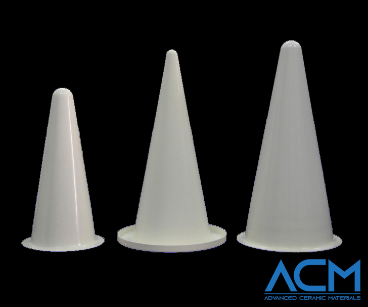
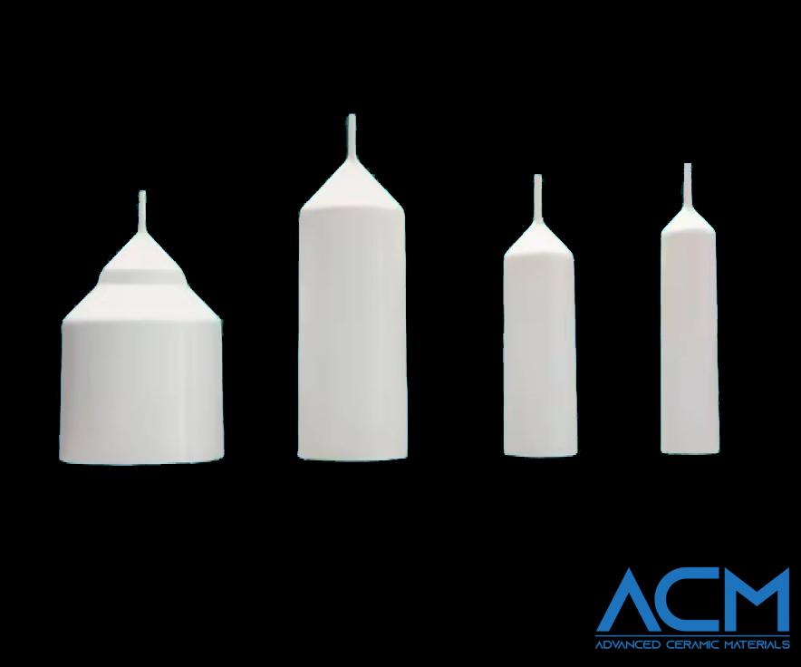
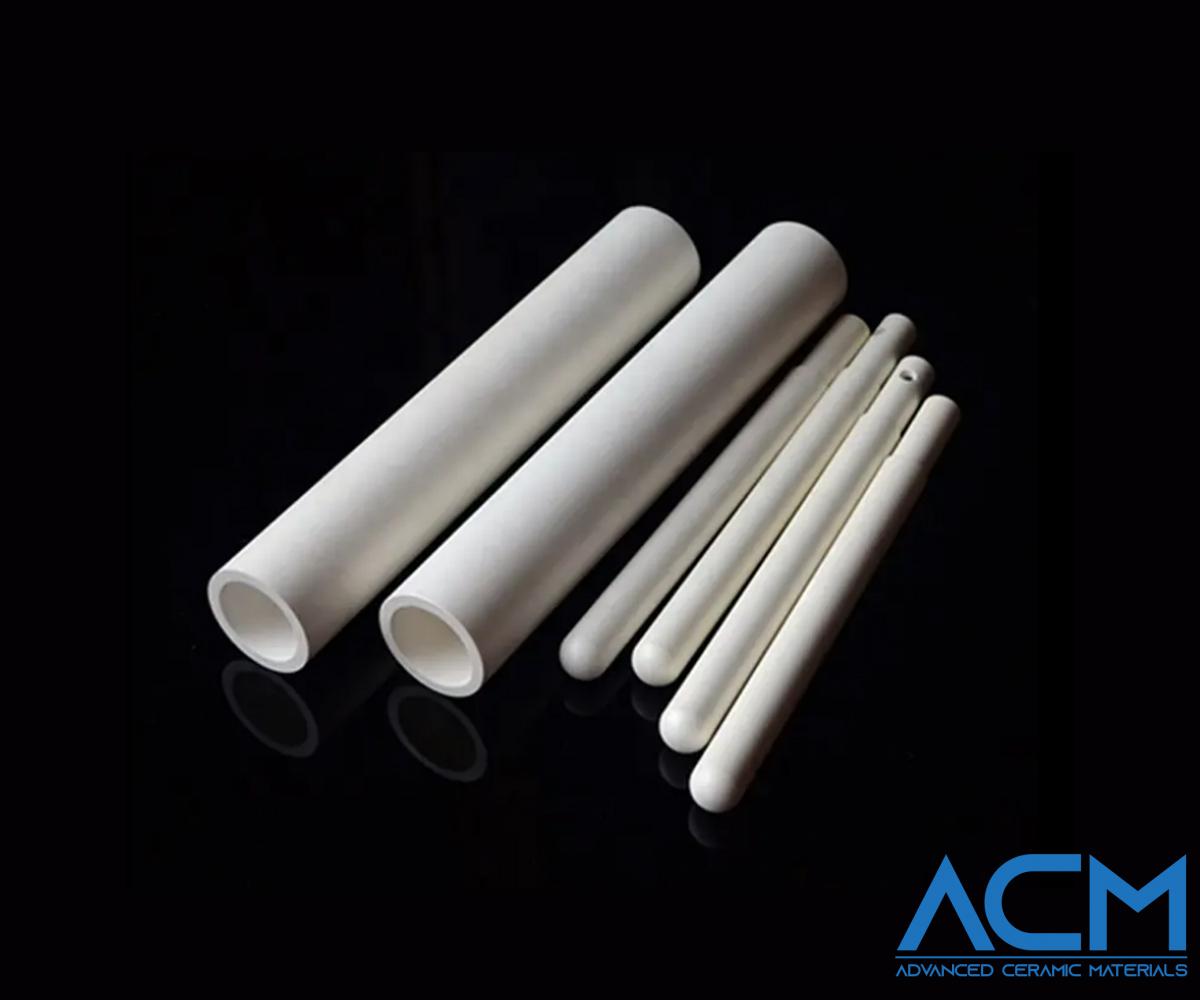
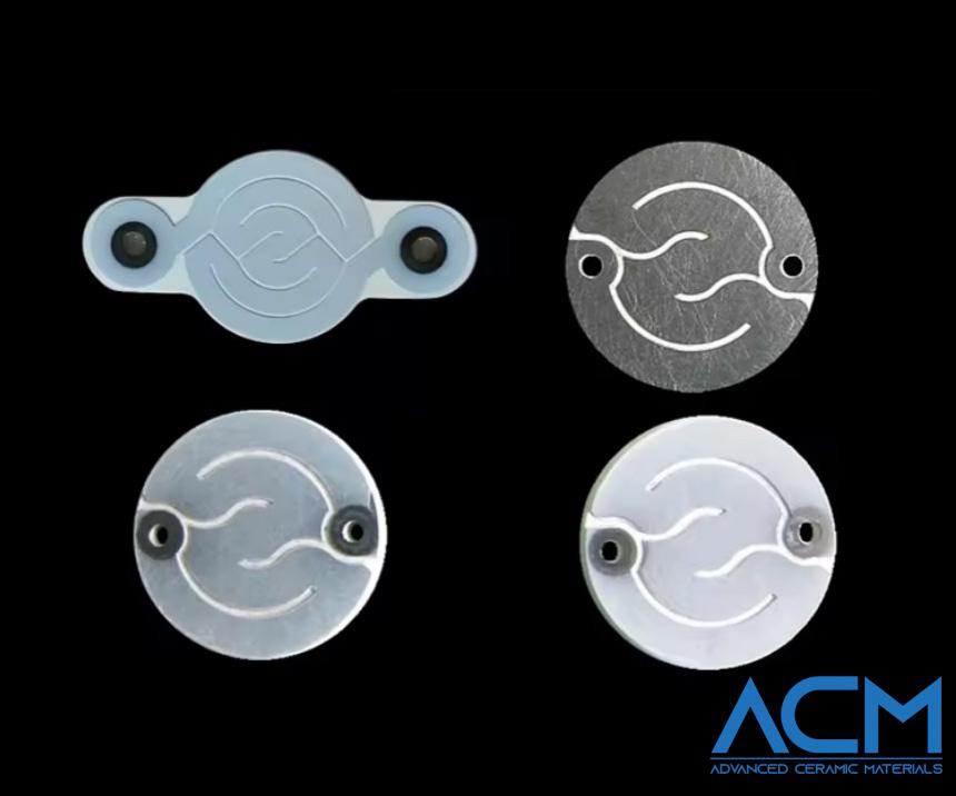
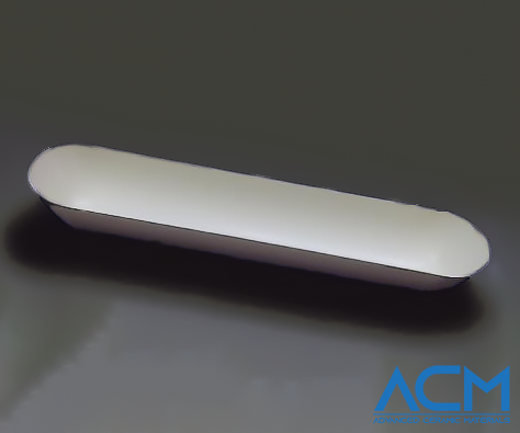
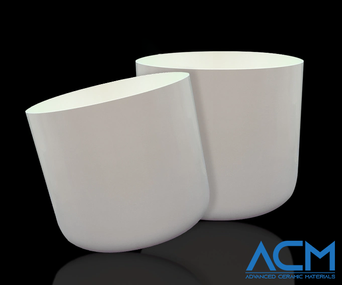
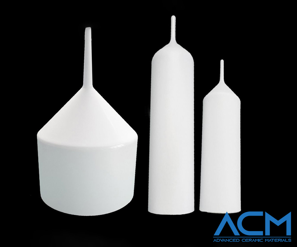
PBN4686 MBE Type Pyrolytic Boron Nitride Crucible
- Catalog No. PBN4686
- Material PBN, Pyrolytic Boron Nitride
- Size Customized
- Density 1.95-2.20 g/cm3
- Purity >99.99%
Datasheet
Inquiry
PBN4686 MBE Type Pyrolytic Boron Nitride Crucible
MBE Type PBN Crucible Description
Pyrolytic Boron Nitride (PBN) represents an advanced ceramic crafted from a high-density powder boasting 99.999% purity. The Pyrolytic Boron Nitride Crucible (MBE Type) is formed through a Chemical Vapor Deposition (CVD) process using BCl3 and NH3 under high-temperature, low-pressure conditions.
MBE Type PBN Crucible Specifications
PBN Mechanical Characteristics
|
Item |
Data |
Unit |
|
Density |
g/cm3 |
1.95-2.20 |
|
Tensile Strength |
MPa |
112 |
|
Bending Strength |
MPa |
173 |
|
Compression Strength |
MPa |
154 |
|
Young's Modulus |
GPa |
18 |
|
Thermal Conductivity (under 1500℃) |
W/m℃ |
"a" 60 "c" 2 |
|
Specific Heat |
J/g·℃ |
0.90 (RT) |
|
Resistivity |
Ω.cm |
2×10¹⁵ |
|
Dielectric Strength |
D.C. volts/mm |
2×10¹⁵ |
|
Dielectric Constant |
- |
"c" 3.07 |
|
Metal Impurity Content |
ppm |
<10 |
Specifications of PBN MBE Crucible
|
Max. Diameter (ID) |
Max. Height |
Thickness |
|
12" |
17" |
customized |
MBE Type Pyrolytic Boron Nitride Crucible Applications
The applications of MBE Type Pyrolytic Boron Nitride Crucible are diverse and integral to advanced material synthesis. Some key applications include:
-
MBE Growth of Epitaxial Layers: The MBE Type Pyrolytic Boron Nitride Crucible is utilized in Molecular Beam Epitaxy processes for the precise growth of epitaxial layers on semiconductor substrates. Its high purity and inert nature contribute to the controlled deposition of thin films with exceptional crystal quality.
-
III-V Compound Semiconductor Research: In the field of semiconductor research, the crucible is employed for the synthesis of III-V compound semiconductors. It plays a crucial role in the growth of materials like GaAs, InP, and other compound semiconductors, ensuring high-quality crystal structures.
-
Quantum Dot Fabrication: MBE processes involving the Pyrolytic Boron Nitride Crucible are instrumental in the fabrication of quantum dots. The crucible provides a clean and controlled environment for the precise deposition of materials, contributing to the development of quantum dot-based technologies.
-
Nanostructure Growth: Researchers use the MBE Type Pyrolytic Boron Nitride Crucible to facilitate the growth of nanostructures. Its inert properties and resistance to contamination make it suitable for creating well-defined nano-sized structures with specific electronic and optical properties.
-
Advanced Semiconductor Device Manufacturing: The crucible finds application in the manufacturing of advanced semiconductor devices. It contributes to the production of high-performance electronic components with tailored properties, meeting the demands of modern technology.
MBE Type PBN Crucible Packaging
Our MBE Type Pyrolytic Boron Nitride Crucible is carefully handled during storage and transportation to preserve the quality of our product in its original condition.
Request a Quote
-
Attachment (Optional)
No file chosen


