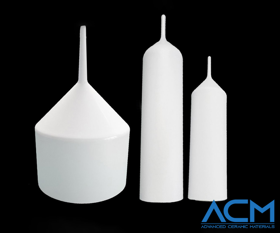
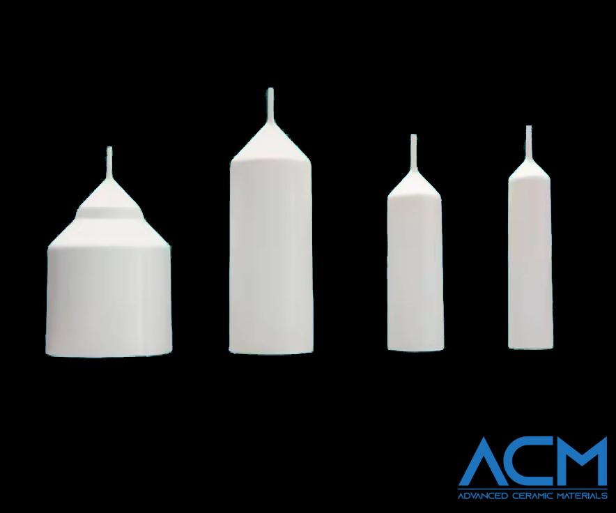
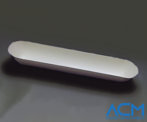
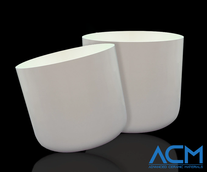
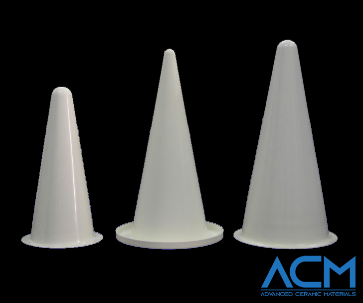
PBN4687 VGF Type Pyrolytic Boron Nitride Crucible
- Catalog No. PBN4687
- Material PBN, Pyrolytic Boron Nitride
- Size Customized
- Density 1.95-2.20 g/cm3
- Purity >99.99%
Datasheet
Inquiry
PBN4687 VGF Type Pyrolytic Boron Nitride Crucible
VGF Type PBN Crucible Description
Pyrolytic Boron Nitride (PBN) represents an advanced ceramic crafted from a high-density powder boasting 99.999% purity. The Pyrolytic Boron Nitride Crucible (VGF Type) is formed through a Chemical Vapor Deposition (CVD) process using BCl3 and NH3 under high-temperature, low-pressure conditions.
VGF Type PBN Crucible Specifications
PBN Mechanical Characteristics
|
Item |
Data |
Unit |
|
Density |
g/cm3 |
1.95-2.20 |
|
Tensile Strength |
MPa |
112 |
|
Bending Strength |
MPa |
173 |
|
Compression Strength |
MPa |
154 |
|
Young's Modulus |
GPa |
18 |
|
Thermal Conductivity (under 1500℃) |
W/m℃ |
"a" 60 "c" 2 |
|
Specific Heat |
J/g·℃ |
0.90 (RT) |
|
Resistivity |
Ω.cm |
2×10¹⁵ |
|
Dielectric Strength |
D.C. volts/mm |
2×10¹⁵ |
|
Dielectric Constant |
- |
"c" 3.07 |
|
Metal Impurity Content |
ppm |
<10 |
Typical Specifications of PBN VGF Crucible
|
Inside Diameter (ID) |
Height |
Thickness |
|
2" |
10" |
0.035" |
|
3" |
10" |
0.035" |
|
4" |
8" |
0.035" |
|
5" |
8" |
0.04" |
|
6" |
7" |
0.04" |
|
8" |
20" |
0.08" |
VGF Type Pyrolytic Boron Nitride Crucible Applications
The VGF Type Pyrolytic Boron Nitride Crucible finds primary applications in the growth of GaAs (Gallium Arsenide) and InP (Indium Phosphide) compound semiconductor single crystals. Here are the key applications:
-
GaAs Single-Crystal Growth: The VGF Type Pyrolytic Boron Nitride Crucible is specifically designed for the controlled growth of GaAs single crystals. GaAs is a vital compound semiconductor widely used in the electronics industry for its applications in high-frequency devices, solar cells, and optoelectronic devices.
-
InP Single-Crystal Growth: The crucible is utilized for the precise growth of InP single crystals. InP is another important compound semiconductor with applications in telecommunications, optical devices, and high-speed electronics. The crucible ensures the production of high-quality InP crystals suitable for various applications.
-
Semiconductor Research and Development: Research laboratories and semiconductor manufacturers leverage the VGF Type Pyrolytic Boron Nitride Crucible for studying and advancing the growth processes of GaAs and InP crystals. It serves as an essential tool in semiconductor research, enabling the exploration of crystal growth techniques and properties.
-
Optoelectronic Device Manufacturing: The crystals grown in the crucible play a pivotal role in the manufacturing of optoelectronic devices. GaAs and InP compounds are integral to the production of lasers, photodetectors, and other optical components used in telecommunications, medical devices, and optical communication systems.
-
High-Performance Electronics: The high-quality single crystals produced using the VGF Type Pyrolytic Boron Nitride Crucible contribute to the manufacturing of high-performance electronic devices. These crystals meet the stringent requirements of the semiconductor industry, ensuring reliable and efficient performance in electronic applications.
VGF Type PBN Crucible Packaging
Our VGF Type Pyrolytic Boron Nitride Crucible is carefully handled during storage and transportation to preserve the quality of our product in its original condition.
Request a Quote
-
Attachment (Optional)
No file chosen


